Born in Vitebsk in 1930. Named in honor of Jean Jaurès, founder of the newspaperL'Humaniteand leader of the French Socialist Party.
He graduated from school with a gold medal and in 1952 graduated from the Faculty of Electronic Engineering of the Leningrad Electrotechnical Institute. IN AND. Ulyanova (LETI).
Since 1953 he worked at the Physico-Technical Institute named after. A.F. Ioffe, took part in the development of the first domestic transistors and germanium power devices. In 1970 he defended his doctoral dissertation, summarizing a new stage of research on heterojunctions in semiconductors. In 1971, he was awarded the first international award - the Stuart Ballantyne Gold Medal of the Franklin Institute (USA), called the Small Nobel Prize.
The Royal Swedish Academy of Sciences awarded Zhores I. Alferov the Nobel Prize in Physics for 2000 - for his work that laid the foundations of modern information technology - for the development of semiconductor heterostructures and the creation of fast opto- and microelectronic components. The development of fiber-optic communications, the Internet, solar energy, mobile telephony, LED and laser technology is largely based on the research and discoveries of Zh.I Alferov.
Also the outstanding contribution of Zh.I. Alferov was awarded numerous international and domestic prizes and awards: Lenin and State Prizes (USSR), Welker Gold Medal (Germany), Kyoto Prize (Japan), A.F. Ioffe, Popov Gold Medal (RAS), State Prize of the Russian Federation, Demidov Prize, Global Energy Prize (Russia), K. Boyer Prize and Gold Medal (USA, 2013) and many others.
Zh.I. Alferov was elected an honorary and foreign member of more than 30 foreign academies of sciences and scientific societies, including national academies of sciences: Italy, Spain, China, Korea and many others. The only Russian scientist who was simultaneously elected as a foreign member of the US National Academy of Sciences and the US National Academy of Engineering. More than 50 universities from 20 countries elected him honorary doctor and professor.
Zh.I. Alferov is a full holder of the Order of Merit for the Fatherland, awarded with state awards of the USSR, Ukraine, Belarus, Cuba, France, and China.
Since 1990 - Vice-President of the USSR Academy of Sciences, since 1991 - Vice-President of the RAS. He is one of the most prominent organizers of academic science in Russia and an active supporter of the creation of educational centers on the basis of leading institutes of the Russian Academy of Sciences. In 1973, at the Physicotechnical Institute, he created the first basic department of optoelectronics at LETI. He was director (1987-2003) and scientific director (2003-2006) of the Physicotechnical Institute. A.F. Ioffe RAS, and since 1988 the dean of the Physics and Technology Faculty of the Leningrad Polytechnic Institute (LPI) created by him. In 2002, he created the Academic University of Physics and Technology - the first higher education institution included in the RAS system. In 2009, the Lyceum “Physical and Technical School” and the Scientific Center for Nanotechnologies, which he created in 1987 on the basis of the Physicotechnical Institute, was annexed to the university and the St. Petersburg Academic University was organized - the scientific and educational center of nanotechnologies of the Russian Academy of Sciences (in 2010 it received the status of National research university), where he became rector. He created his own scientific school: among his students there are more than 50 candidates, dozens of doctors of science, 7 corresponding members of the Russian Academy of Sciences. Since 2010 - co-chairman, together with Nobel laureate Roger Kornberg (USA), of the Scientific Advisory Council of the Skolkovo Foundation.
In February 2001, he created the Foundation for the Support of Education and Science (Alferov Foundation), investing a significant part of his Nobel Prize into it. The foundation's first charitable program is “Establishment of lifelong financial assistance to widows of academicians and corresponding members of the Russian Academy of Sciences who worked in St. Petersburg.” The Foundation has established scholarships for students of Russian schools and lyceums, university students and graduate students, prizes and grants for young scientists. In a number of countries there are representative offices and independent funds for the support of education and science, established by Zh.I. Alferov and created with his assistance: in the Republic of Belarus, in Kazakhstan, in Italy, in Ukraine, in Azerbaijan.
Zhores Alferov is a living legend of Russian science. A scientist whose discoveries became the basis for the creation of modern electronic devices. It is no longer possible to imagine our world without lasers, semiconductors, LEDs and fiber optic networks. All this became available to humanity thanks to the inventions of Zhores Alferov and the young scientists he trained.
The merits of the Russian (formerly Soviet) physicist are highly noted in all corners of the Earth and even in space. Asteroid (3884) Alferov is named after a Nobel Prize laureate, academician of the Russian Academy of Sciences and an honorary member of international scientific communities.
Childhood and youth
The scientist's childhood fell on difficult years. The world has changed a lot since the youngest son was born into the family of communists Ivan Karpovich Alferov and Anna Vladimirovna Rosenblum. The parents named their eldest son Marx (he died in the last days of the Korsun-Shevchenko battle), and the youngest was named in honor of Jean Jaurès, the leader of the French socialists.
Family of Zhores Alferov: parents and brother
Born on March 15, 1930 in Vitebsk, before the war the child managed to travel with his parents to the construction sites of Stalingrad, Novosibirsk, Barnaul and Syasstroy. If the Alferov family had remained to live in Belarus, then world science could have suffered a huge loss without ever knowing about him. Anna Rosenblum's nationality would have caused the death of both mother and son at the hands of the Nazis.

During the Second World War, the family lived in the Sverdlovsk region, but the future scientist did not have the opportunity to study normally at school at that time. However, upon returning to Minsk, Zhores quickly made up for lost time. I graduated from school with a gold medal. Now this school is called gymnasium No. 42 and bears the name of the famous student.
Physics teacher Yakov Borisovich Meltzerzon noticed the young man’s abilities and recommended enrolling in the energy department of the Belarusian Polytechnic University. Having decided on his range of scientific interests, Alferov transferred to LETI. In 1952 he began his scientific career.
The science
The graduate dreamed of working at the Physics and Technology Institute under the leadership of Abram Fedorovich Ioffe. The Institute of Physics and Technology was a legend in the post-war period. It was jokingly called “Ioffe’s kindergarten” - it was there that young people grew up. There Zhores Ivanovich became part of the team that created the first Soviet transistors.

Transistors became the topic for the young scientist’s Ph.D. thesis. Subsequently, Zhores Ivanovich switched to the study of heterostructures (artificial crystals) and the movement of light and other types of radiation in them. His laboratory worked with lasers, and already in 1970 they created the world's first solar cells. They equipped satellites and supplied electricity to the Mir orbital station.
Applied science classes went in parallel with teaching work. Zhores Ivanovich wrote books and articles. He headed the department of optoelectronics and personally selected students. Schoolchildren keen on physics attended his annual lecture courses “Physics and Life”.

Nowadays, at the Academic University, whose permanent rector is Zhores Alferov, there is a lyceum “Physical and Technical School”. The lyceum is the lower level of a scientific and educational institution, which also includes a powerful research center. The academician sees the future of Russian science in lyceum students.
“The future of Russia is science and technology, not the sale of raw materials. And the future of the country does not belong to the oligarchs, but to one of my students.”
This quote from a public speech by Zhores Ivanovich reveals the scientist’s belief in the victory of an inquisitive mind over the desire for enrichment.
Personal life
Perhaps the scientist’s first scientific successes were facilitated by failure in his personal life. Zhores Ivanovich's first marriage broke up with scandal. The beautiful wife, with the help of influential Georgian relatives, sued her Leningrad apartment from her husband during the divorce. Alferov owned only a motorcycle and a cot on which he spent the night in the laboratory. The breakdown of the relationship resulted in a complete loss of the father-daughter relationship.

The scientist remarried only in 1967, and this marriage has stood the test of time. Together with Tamara Darskaya, Zhores raised her daughter Irina and their common son Ivan. The birth of his son coincided with another event in his biography - receiving the Lenin Prize. The children have grown up long ago, Zhores Ivanovich managed to become a grandfather. He has two grandchildren and a granddaughter.
Last years
The scientist’s authority in world science rests on more than 500 scientific works and almost a hundred inventions. But the Nobel laureate’s activities were not limited to physics. In the summer of 2017, within the walls of Samara University, the academician gave an open lecture on the topic: “Albert Einstein, socialism and the modern world,” where he discussed issues of interaction between scientists and rulers.

In his speeches, the scientist called the situation of science in Russia appalling and defended the rights of the Russian Academy of Sciences to self-government and decent funding. The scientist believed that the state should provide citizens with free medicine, education and housing, and otherwise this structure is useless.
Zhores Ivanovich was directly involved in governing the state. Back in 1989, he was elected People's Deputy of the USSR from the Academy of Sciences. Since then, the academician has been constantly elected to the Russian Duma, actively defending the interests of scientists and ordinary citizens.

In August 2017, Forbes magazine included Zhores Alferov among the hundred most influential Russians of the last century. Despite his advanced age, the Nobel laureate looked cheerful and confident in the videos and photos.
Death
March 2, 2019 Zhores Alferov at the age of 88 years. As Oleg Chagunava, the head physician of the hospital of the Russian Academy of Sciences, told reporters, the cause of death of the Nobel laureate was acute cardiopulmonary failure. The day before, Alferov was observed by doctors for several months with a complaint of hypertension.
The Communist Party of the Russian Federation took over the organization of the funeral of the famous physicist.
Awards and achievements
- 1959 - Order of the Badge of Honor
- 1971 - Stuart Ballantyne Medal (USA)
- 1972 - Lenin Prize
- 1975 - Order of the Red Banner of Labor
- 1978 - Hewlett-Packard Prize (European Physical Society)
- 1980 - Order of the October Revolution
- 1984 - USSR State Prize
- 1986 - Order of Lenin
- 1987 - Heinrich Welker Gold Medal (GaAs Symposium)
- 1989 - Karpinsky Prize (Germany)
- 1993 - XLIX Mendeleev's reader
- 1996 - A.F. Ioffe Prize (RAS)
- 1998 - Honorary Doctor of St. Petersburg State Unitary Enterprise
- 1999 - Order of Merit for the Fatherland, III degree
- 1999 - Demidov Prize (Scientific Demidov Foundation)
- 1999 - Gold medal named after A. S. Popov (RAN)
- 2000 - Nobel Prize (Sweden)
- 2000 - Order of Merit for the Fatherland, II degree
- 2000 - Nick Holonyak Award (Optical Society of America)
- 2001 - Order of Francis Skaryna (Belarus)
- 2001 - Kyoto Prize (Japan)
- 2001 - V. I. Vernadsky Prize (Ukraine)
- 2001 - Russian National Olympus Award. Title "Man-Legend"
- 2002 - State Prize of the Russian Federation
- 2002 - SPIE Gold Medal
- 2002 - Golden Plate Award (USA)
- 2003 - Order of Prince Yaroslav the Wise, V degree (Ukraine)
- 2005 - Order of Merit for the Fatherland, 1st degree
- 2005 - International Energy Prize "Global Energy"
- 2008 - Title and medal of Honorary Professor of MIPT
- 2009 - Order of Friendship of Peoples (Belarus)
- 2010 - Order of Merit for the Fatherland, IV degree
- 2010 - Medal “For contribution to the development of nanoscience and nanotechnology” from UNESCO
- 2011 - Title “Honorary Doctor of the Russian-Armenian (Slavic) University”
- 2013 - International Karl Boer Prize
- 2015 - Order of Alexander Nevsky
- 2015 - Gold medal named after Nizami Ganjavi (Azerbaijan)
- 2015 - Title “Honorary Professor of MIET”
In March of this year, Academician Zhores Ivanovich Alferov, Nobel laureate and member of the editorial board of the journal Ecology and Life, turned 80 years old. And in April, the news came that Zhores Ivanovich was appointed scientific director of the Skolkovo innovation project. This important project should, in fact, create a breakthrough into the future, breathing new life into domestic electronics, the origins of which were Zh. I. Alferov.
History speaks in favor of the fact that a breakthrough is possible: when the first satellite was launched in the USSR in 1957, the United States found itself in the position of an outsider. However, the American government showed a militant character, such investments were made into technology that the number of researchers quickly reached a million! Literally the next year (1958), one of them, John Kilby, invented an integrated circuit that replaced the printed circuit board in conventional computers - and the microelectronics of modern computers was born. This story later became known as the “satellite effect.”
Zhores Ivanovich is very attentive to the education of future researchers; it is not for nothing that he founded a REC - a training center where training is carried out from school. Congratulating Zhores Ivanovich on his anniversary, let's look into the past and future of electronics, where the satellite effect should appear again more than once. I would like to hope that in the future our country, as once in the United States, will accumulate a “critical mass” of trained researchers for the satellite effect to occur.
"Technical" light
The first step towards the creation of microelectronics was the transistor. The pioneers of the transistor era were William Shockley, John Bardeen and Walter Brattain, who in 1947 in “ Bell Labs"For the first time, a functioning bipolar transistor was created. And the second component of semiconductor electronics was a device for directly converting electricity into light - this is a semiconductor optoelectronic converter, to the creation of which Zh. I. Alferov was directly involved.
The problem of direct conversion of electricity into “technical” light - coherent quantum radiation - took shape as a direction in quantum electronics, born in 1953–1955. In essence, scientists have posed and solved the problem of obtaining a completely new type of light, which had not previously existed in nature. This is not the kind of light that flows in a continuous stream when a current passes through a tungsten filament, or comes during the day from the Sun and consists of a random mixture of waves of different lengths, out of phase. In other words, strictly “dosed” light was created, obtained as a set of a certain number of quanta with a given wavelength and strictly “constructed” - coherent, i.e. ordered, which means the simultaneity (in phase) of the radiation of the quanta.
The US priority for the transistor was determined by the huge burden of the Patriotic War that fell on our country. Zhores Ivanovich’s older brother, Marks Ivanovich, died in this war.

Marx Alferov graduated from school on June 21, 1941 in Syasstroy. He entered the Ural Industrial Institute at the Faculty of Energy, but studied for only a few weeks, and then decided that his duty was to defend his homeland. Stalingrad, Kharkov, Kursk Bulge, severe wound to the head. In October 1943, he spent three days with his family in Sverdlovsk, when he returned to the front after hospitalization.
13-year-old Jaures remembered the three days spent with his brother, his stories from the front and his passionate youthful belief in the power of science and engineering for the rest of his life. Guard junior lieutenant Marx Ivanovich Alferov died in battle in the “second Stalingrad” - that’s what the Korsun-Shevchenko operation was called then.
In 1956, Zhores Alferov came to Ukraine to find his brother’s grave. In Kyiv, on the street, he unexpectedly met his colleague B.P. Zakharchenya, who later became one of his closest friends. We agreed to go together. We bought tickets for the ship and the very next day we sailed down the Dnieper to Kanev in a double cabin. We found the village of Khilki, near which Soviet soldiers, including Marx Alferov, repelled a furious attempt by selected German divisions to leave the Korsun-Shevchenko “cauldron”. We found a mass grave with a white plaster soldier on a pedestal rising above lush grass, interspersed with simple flowers, the kind usually planted on Russian graves: marigolds, pansies, forget-me-nots.
By 1956, Zhores Alferov was already working at the Leningrad Institute of Physics and Technology, where he dreamed of going while still studying. A major role in this was played by the book “Basic Concepts of Modern Physics,” written by Abram Fedorovich Ioffe, the patriarch of Russian physics, from whose school came almost all the physicists who later became the pride of the Russian physics school: P. L. Kapitsa, L. D. Landau, I. V. Kurchatov, A. P. Alexandrov, Yu. B. Khariton and many others. Zhores Ivanovich wrote much later that his happy life in science was predetermined by his assignment to the Phystech, which later received the name Ioffe.
Systematic research on semiconductors at the Institute of Physics and Technology began back in the 30s of the last century. In 1932, V. P. Zhuze and B. V. Kurchatov investigated the intrinsic and impurity conductivity of semiconductors. In the same year, A.F. Ioffe and Ya.I. Frenkel created a theory of current rectification at a metal-semiconductor contact, based on the phenomenon of tunneling. In 1931 and 1936, Ya. I. Frenkel published his famous works, in which he predicted the existence of excitons in semiconductors, introducing this term and developing the theory of excitons. The theory of the rectifying p–n junction, which formed the basis for the p–n junction of V. Shockley, who created the first transistor, was published by B. I. Davydov, an employee of the Fiztekh, in 1939. Nina Goryunova, a graduate student of Ioffe, who defended in 1950. dissertation on intermetallic compounds, discovered the semiconductor properties of compounds of the 3rd and 5th groups of the periodic table (hereinafter A 3 B 5). It was she who created the foundation on which research into the heterostructures of these elements began. (In the West, G. Welker is considered the father of semiconductors A 3 B 5.)
Alferov himself did not have the opportunity to work under the leadership of Ioffe - in December 1950, during the campaign to “fight cosmopolitanism,” Ioffe was removed from the post of director and removed from the Academic Council of the institute. In 1952, he headed the semiconductor laboratory, on the basis of which the Institute of Semiconductors of the USSR Academy of Sciences was organized in 1954.
Alferov submitted an application for the invention of a semiconductor laser together with theorist R.I. Kazarinov at the height of the search for a semiconductor laser. These searches have been going on since 1961, when N. G. Basov, O. N. Krokhin and Yu. M. Popov formulated the theoretical prerequisites for its creation. In July 1962, the Americans decided on a semiconductor for lasing - it was gallium arsenide, and in September-October the laser effect was obtained in three laboratories at once, the first was Robert Hall's group (September 24, 1962). And five months after Hall’s publication, an application for the invention of Alferov and Kazarinov was submitted, from which the study of heterostructure microelectronics at the Physics and Technology Institute began.

Alferov's group (Dmitry Tretyakov, Dmitry Garbuzov, Efim Portnoy, Vladimir Korolkov and Vyacheslav Andreev) struggled for several years to find a material suitable for implementation, trying to make it themselves, but found a suitable complex three-component semiconductor almost by accident: in the neighboring laboratory of N. A. Goryunova . However, this was a “non-random” accident - Nina Aleksandrovna Goryunova conducted a targeted search for promising semiconductor compounds, and in a monograph published in 1968, she formulated the idea of a “periodic system of semiconductor compounds.” The semiconductor compound created in her laboratory had the stability necessary for generation, which determined the success of the “enterprise.” A heterolaser based on this material was created on the eve of 1969, and the priority date for detecting the laser effect is September 13, 1967.
New materials
Against the backdrop of the laser race that had unfolded since the early 60s, LEDs almost imperceptibly emerged, which also produced light of a given spectrum, but did not have the strict coherence of a laser. As a result, today's microelectronics includes such basic functional devices as transistors and their conglomerates - integrated circuits (thousands of transistors) and microprocessors (from tens of thousands to tens of millions of transistors), while in fact a separate branch of microelectronics - optoelectronics - consisted of devices built on the basis heterostructures for creating “technical” light - semiconductor lasers and LEDs. The recent history of digital recording is connected with the use of semiconductor lasers - from ordinary CDs to the technology famous today Blue Ray on gallium nitride (GaN).
Light-emitting diode, or light-emitting diode (LED, LED, LED - English. Light-emitting diode), is a semiconductor device that emits incoherent light when an electric current is passed through it. The emitted light lies in a narrow range of the spectrum, its color characteristics depend on the chemical composition of the semiconductor used in it.
The first LED emitting light in the visible range is believed to have been manufactured in 1962 at the University of Illinois by a team led by Nick Holonyak. Diodes made from indirect gap semiconductors (for example, silicon, germanium or silicon carbide) emit virtually no light. Therefore, materials such as GaAs, InP, InAs, InSb, which are direct-gap semiconductors, were used. At the same time, many semiconductor materials of type A 3 B E form among themselves a continuous series of solid solutions - ternary and more complex (AI x Ga 1- x N and In x Ga 1- x N,GaAs x P 1- x,Ga x In 1- x P,Ga x In 1- x As y P 1- y etc.), on the basis of which the direction of heterostructure microelectronics was formed.
The most well-known use of LEDs today is replacing incandescent lamps and displays of mobile phones and navigators.
The general idea for the further development of “technical light” is the creation of new materials for LED and laser technology. This task is inseparable from the problem of obtaining materials with certain requirements for the electronic structure of the semiconductor. And the main one of these requirements is the structure of the band gap of the semiconductor matrix used to solve a particular problem. Active research is being carried out on combinations of materials that make it possible to achieve specified requirements for the shape and size of the band gap.
You can get an idea of the versatility of this work by looking at the graph, which allows you to evaluate the variety of “basic” double compounds and the possibilities of their combinations in composite heterostructures.
We welcome thousands of suns!
The history of technical light would be incomplete if, along with light emitters, there was no development of light receivers. If the work of Alferov’s group began with the search for material for emitters, then today one of the members of this group, Alferov’s closest collaborator and his longtime friend Professor V.M. Andreev is closely involved in work related to the reverse transformation of light, and precisely the transformation that is used in solar cells. The ideology of heterostructures as a complex of materials with a given band gap has found active application here too. The fact is that sunlight consists of a large number of light waves of different frequencies, which is precisely the problem of its full use, since there is no material that could equally convert light of different frequencies into electrical energy. It turns out that any silicon solar battery does not convert the entire spectrum of solar radiation, but only part of it. What to do? The “recipe” is deceptively simple: make a layer cake from various materials, each layer of which responds to a different frequency, but at the same time allows all other frequencies to pass through without significant attenuation.
This is an expensive structure, since it must contain not only transitions of different conductivity on which light falls, but also many auxiliary layers, for example, so that the resulting EMF can be removed for further use. Essentially, a “sandwich” assembly of several electronic devices. Its use is justified by the higher efficiency of “sandwiches,” which can be effectively used in conjunction with a solar concentrator (lens or mirror). If a “sandwich” allows you to increase the efficiency compared to a silicon element, for example, by 2 times - from 17 to 34%, then due to a concentrator that increases the density of solar radiation by 500 times (500 suns), you can get a gain of 2 × 500 = 1000 times! This is a gain in the area of the element itself, i.e., 1000 times less material is needed. Modern solar radiation concentrators measure radiation density in thousands and tens of thousands of “suns” concentrated on a single element.

Another possible way is to obtain a material that can operate at least at two frequencies, or more precisely, with a wider range of the solar spectrum. In the early 1960s, the possibility of a “multizone” photoelectric effect was demonstrated. This is a peculiar situation where the presence of impurities creates bands in the band gap of the semiconductor, which allows electrons and holes to “jump across the gap” in two or even three jumps. As a result, it is possible to obtain a photoelectric effect for photons with a frequency of 0.7, 1.8 or 2.6 eV, which, of course, significantly expands the absorption spectrum and increases the efficiency. If scientists manage to ensure generation without significant recombination of carriers in the same impurity bands, then the efficiency of such elements can reach 57%.
Since the early 2000s, active research has been conducted in this direction under the leadership of V. M. Andreev and Zh. I. Alferov.
There is another interesting direction: the flow of sunlight is first split into flows of different frequency ranges, each of which is then sent to its “own” cells. This direction can also be considered promising, since this eliminates the series connection, inevitable in “sandwich” structures like the one shown above, which limits the element current to the “weakest” (at this time of day and on this material) part of the spectrum.
Of fundamental importance is the assessment of the relationship between solar and nuclear energy, expressed by Zh. I. Alferov at one of the recent conferences: “If only 15% of the funds allocated for the development of nuclear energy were spent on the development of alternative energy sources, then nuclear power plants for the production of electricity in the USSR wouldn’t be needed at all!”
The future of heterostructures and new technologies
Another assessment is also interesting, reflecting the point of view of Zhores Ivanovich: in the 21st century, heterostructures will leave only 1% for the use of monostructures, i.e. all electronics will move away from such “simple” substances as silicon with a purity of 99.99–99.999%. The numbers are the purity of silicon, measured in nines after the decimal point, but this purity has not surprised anyone for 40 years. The future of electronics, Alferov believes, is compounds of elements A 3 B 5, their solid solutions and epitaxial layers of various combinations of these elements. Of course, it cannot be said that simple semiconductors such as silicon cannot find wide application, but still complex structures provide a much more flexible answer to the needs of our time. Already today, heterostructures solve the problem of high information density for optical communication systems. We are talking about OEIC ( optoelectronic integrated circuit) - optoelectronic integrated circuit. The basis of any optoelectronic integrated circuit (optocoupler, optocoupler) is an infrared emitting diode and an optically matched radiation receiver, which gives scope to formal circuitry for the widespread use of these devices as information transceivers.
In addition, the key device of modern optoelectronics - the DGS laser (DGS - double heterostructure) - continues to be improved and developed. Finally, today it is high-efficiency, high-speed heterostructure LEDs that provide support for high-speed data transmission technology HSPD ( High Speed Packet Data service).
But the most important thing in Alferov’s conclusion is not these isolated applications, but the general direction of development of technology of the 21st century - the production of materials and integrated circuits based on materials that have precisely specified properties designed for many moves ahead. These properties are set through design work, which is carried out at the level of the atomic structure of the material, determined by the behavior of charge carriers in that special regular space, which represents the inside of the crystal lattice of the material. In essence, this work is regulating the number of electrons and their quantum transitions - jewelry work at the level of constructing a constant crystal lattice, which is several angstroms in size (angstroms - 10–10 m, 1 nanometer = 10 angstroms). But today the development of science and technology is no longer the path into the depths of matter as it was imagined in the 60s of the last century. Today, much of this is moving in the opposite direction, into the nanoscale region - for example, creating nanoregions with the properties of quantum dots or quantum wires, where the quantum dots are linearly connected.
Naturally, nanoobjects are just one of the stages that science and technology go through in their development, and they will not stop there. It must be said that the development of science and technology is far from a straightforward path, and if today the interests of researchers have shifted towards increasing sizes - into the nanoarea, then tomorrow's solutions will compete on different scales.
For example, restrictions on further increasing the density of microcircuit elements that have arisen on silicon chips can be solved in two ways. The first way is to change the semiconductor. For this purpose, a variant has been proposed for the manufacture of hybrid microcircuits based on the use of two semiconductor materials with different characteristics. The most promising option is the use of gallium nitride in conjunction with a silicon wafer. On the one hand, gallium nitride has unique electronic properties that make it possible to create high-speed integrated circuits; on the other hand, the use of silicon as a basis makes this technology compatible with modern production equipment. However, the nanomaterials approach contains an even more innovative idea of single-electron electronics - single-electronics.
The fact is that further miniaturization of electronics - placing thousands of transistors on the substrate of one microprocessor - is limited by the intersection of electric fields during the movement of electron flows in nearby transistors. The idea is to instead of streams of electrons, use a single electron, which can move on an "individual" time schedule and therefore does not create "queues", thereby reducing the intensity of interference.
If you look at it, electron flows, in general, are not needed - to transfer control, you can give as small a signal as you like, the problem is to confidently isolate (detect) it. And it turns out that single-electron detection is technically quite feasible - for this, the tunnel effect is used, which is an individual event for each electron, in contrast to the usual movement of electrons “in the general mass” - the current in a semiconductor is a collective process. From an electronics point of view, a tunnel junction is the transfer of charge through a capacitor, therefore, in a field-effect transistor, where the capacitor is at the input, a single electron can be “caught” by the oscillation frequency of the amplified signal. However, it was possible to isolate this signal in conventional devices only at cryogenic temperatures - an increase in temperature destroyed the conditions for detecting the signal. But the temperature at which the effect disappears turned out to be inversely proportional to the contact area, and in 2001 it was possible to make the first single-electron transistor on a nanotube, in which the contact area was so small that it allowed operation at room temperatures!
In this regard, single-electronics follows the path taken by researchers of semiconductor heterolasers - Alferov’s group was struggling to find a material that would provide the laser lasing effect at room temperature, and not at the temperature of liquid nitrogen. But superconductors, with which the greatest hopes are associated with transmitting large flows of electrons (power currents), have not yet been able to be “pulled” out of the cryogenic temperature region. This not only significantly impedes the possibility of reducing losses when transmitting energy over long distances - it is well known that redirecting energy flows across Russia during the day leads to 30% losses due to “heating of wires”, - the lack of “indoor” superconductors limits the development of storage energy in superconducting rings, where the flow of current can continue almost forever. The so far unattainable ideal for creating such rings is provided by ordinary atoms, where the movement of electrons around the nucleus is sometimes stable at the highest temperatures and can continue indefinitely.
Future prospects for the development of materials science are very diverse. Moreover, it was with the development of materials science that a real possibility of direct use of solar energy appeared, promising enormous prospects for renewable energy. Sometimes it is precisely these areas of work that determine the future face of society (in Tatarstan and Chuvashia they are already planning a “green revolution” and are seriously developing the creation of bioeco-cities). Perhaps the future of this direction is to move from the development of materials technology to understanding the principles of the functioning of nature itself, to take the path of using controlled photosynthesis, which can be distributed in human society as widely as in living nature. We are already talking about an elementary cell of living nature - a cell, and this is the next, higher stage of development after electronics with its ideology of creating devices to perform a single function - a transistor to control current, an LED or laser to control light. The ideology of the cell is the ideology of operators as elementary devices that carry out a certain cycle. The cell does not serve as an isolated element for performing any one function at the expense of external energy, but as an entire factory for processing available external energy into the work of maintaining cycles of many different processes under a single shell. The work of a cell to maintain its own homeostasis and accumulate energy in it in the form of ATP is an exciting problem of modern science. For now, biotechnologists can only dream of creating an artificial device with the properties of a cell, suitable for use in microelectronics. And when this happens, undoubtedly, a new era of microelectronics will begin - an era of approaching the principles of operation of living organisms, an old dream of science fiction writers and the long-invented science of bionics, which has not yet emerged from the cradle of biophysics.
Let's hope that the creation of a scientific center for innovation in Skolkovo will be able to realize something similar to the “sputnik effect” - to open new breakthrough areas, create new materials and electronics technologies.
We wish success to Zhores Ivanovich Alferov in his post as scientific director of this new scientific and technological agglomerate. It is hoped that his energy and perseverance will be the key to the success of this enterprise.
The band gap is a region of energy values that cannot be possessed by an electron in an ideal (defect-free) crystal. The characteristic values of the band gap in semiconductors are 0.1–4 eV. Impurities can create bands in the bandgap - a multiband occurs.
Born on March 15, 1930 in Vitebsk in the family of Ivan Karpovich and Anna Vladimirovna Alferov, natives of Belarus. The father of an eighteen-year-old boy came to St. Petersburg in 1912. He worked as a loader at the port, as a laborer at an envelope factory, and as a worker at the Lessner plant (later the Karl Marx Plant). During World War I he rose to the rank of non-commissioned officer in the Life Guards, becoming a Knight of St. George.
In September 1917, I.K. Alferov joined the Bolshevik Party and remained faithful to the ideals chosen in his youth for the rest of his life. This, in particular, is evidenced by the bitter words of Zhores Ivanovich himself: “I am happy that my parents did not live to see this time” (1994). During the civil war, I.K. Alferov commanded a cavalry regiment of the Red Army, met with V.I. Lenin, L.D. Trotsky, B.B. Dumenko. After graduating from the Industrial Academy in 1935, he went from plant director to head of the trust: Stalingrad, Novosibirsk, Barnaul, Syasstroy (near Leningrad), Turinsk (Sverdlovsk region, war years), Minsk (after the war). Ivan Karpovich was characterized by internal decency and intolerance to indiscriminate condemnation of people.
Anna Vladimirovna had a clear mind and great worldly wisdom, largely inherited by her son. She worked in the library and headed the council of social wives.

Zh.I. Alferov with his parents, Anna Vladimirovna and Ivan Karpovich (1954).
The couple, like most people of that generation, staunchly believed in revolutionary ideas. Then the fashion arose to give children sonorous revolutionary names. The younger son became Jaurès in honor of the French revolutionary Jean Jaurès, and the eldest son became Marx, in honor of the founder of scientific communism. Jaurès and Marx were the director's children, which means they had to be an example both in their studies and in public life.
The Moloch of repression bypassed the Alferov family, but the war took its toll. Marx Alferov graduated from school on June 21, 1941 in Syasstroy. He entered the Ural Industrial Institute at the Faculty of Energy, but studied for only a few weeks, and then decided that his duty was to defend his homeland. Stalingrad, Kharkov, Kursk Bulge, severe wound to the head. In October 1943, he spent three days with his family in Sverdlovsk, when he returned to the front after hospitalization. And Zhores remembered these three days, the front-line stories of his older brother, his passionate youthful faith in the power of science and engineering for the rest of his life. Guard junior lieutenant Marx Ivanovich Alferov died in battle in the “second Stalingrad” - that’s what the Korsun-Shevchenkovsky operation was called then.

In 1956, Zhores came to Ukraine to find his brother’s grave. In Kyiv, on the street, he unexpectedly met his colleague B.P. Zakharchenya, who later became one of his closest friends. We agreed to go together. We bought tickets for the ship and the very next day we sailed down the Dnieper to Kanev in a double cabin. We found the village of Khilki, near which Marx Alferov fiercely repelled the attempt of selected German divisions to leave the Korsun-Shevchenko “cauldron”. We found a mass grave with a white plaster soldier on a pedestal rising above lush grass, interspersed with simple flowers, the kind usually planted on Russian graves: marigolds, pansies, forget-me-nots.
In destroyed Minsk, Zhores studied at the only Russian male secondary school No. 42 at that time, where there was a wonderful physics teacher - Yakov Borisovich Meltzerzon. The school did not have a physics classroom, but Yakov Borisovich, who was in love with physics, knew how to convey to his students his attitude towards his favorite subject, so there was never any mischief in the rather hooligan class. Zhores, amazed by Yakov Borisovich's story about the operation of a cathode oscilloscope and the principles of radar, went in 1947 to study in Leningrad, at the Electrotechnical Institute, although his gold medal opened up the possibility of admission to any institute without exams. Leningrad Electrotechnical Institute (LETI) named after. V.I. Ulyanov (Lenin) was an institution with a unique name: it mentioned both the real name and the party nickname of a person whom part of the population of the former USSR now does not really respect (now it is the St. Petersburg State Electrotechnical University).
The foundation of science at LETI, which played an outstanding role in the development of domestic electronics and radio engineering, was laid by such “whales” as Alexander Popov, Genrikh Graftio, Axel Berg, Mikhail Chatelain. Zhores Ivanovich, according to him, was very lucky with his first scientific supervisor. In his third year, believing that mathematics and theoretical disciplines were easy, and that he needed to learn a lot “with his hands,” he went to work in the vacuum laboratory of Professor B.P. Kozyrev. There, having begun experimental work in 1950 under the guidance of Natalia Nikolaevna Sozina, who had recently defended her dissertation on the study of semiconductor photodetectors in the IR region of the spectrum, Zh.I. Alferov first encountered semiconductors, which became the main work of his life. The first monograph on semiconductor physics studied was F.F. Volkenshtein’s book “Electrical Conductivity of Semiconductors,” written during the siege of Leningrad. In December 1952, distribution took place. Zh.I. Alferov dreamed of a Phystech, headed by Abram Fedorovich Ioffe, whose monograph “Basic Concepts of Modern Physics” became a reference book for the young scientist. During the distribution, there were three vacancies, and one went to Zh.I. Alferov. Zhores Ivanovich wrote much later that his happy life in science was predetermined precisely by this distribution. In a letter to his parents in Minsk, he reported on his great happiness to work at the Ioffe Institute. Zhores did not yet know that Abram Fedorovich, two months earlier, had been forced to leave the institute he had created, where he had been director for more than 30 years.
Systematic research on semiconductors at the Institute of Physics and Technology began back in the 30s. last century. In 1932, V.P. Zhuze and B.V. Kurchatov investigated the intrinsic and impurity conductivity of semiconductors. In the same year, A.F. Ioffe and Ya.I. Frenkel created a theory of current rectification at a metal-semiconductor contact, based on the phenomenon of tunneling. In 1931 and 1936 Ya.I. Frenkel published his famous works, in which he predicted the existence of excitons in semiconductors, introducing this term itself and developing the theory of excitons. The first diffusion theory of rectifier p–n-transition, which became the basis of the theory p–n-transition by V. Shockley, was published by B.I. Davydov in 1939. On the initiative of A.F. Ioffe from the late 40s. Research into intermetallic compounds began at the Physics and Technology Institute.
On January 30, 1953, Zh.I. Alferov began working with a new scientific supervisor, at that time the head of the sector, candidate of physical and mathematical sciences Vladimir Maksimovich Tuchkevich. A small team in the sector was given a very important task: the creation of the first domestic germanium diodes and transistors with p–n junctions (see “Physics” No. 40/2000, V.V.Randoshkin. Transistor). The topic “Plane” was entrusted by the government in parallel to four institutes: FIAN and Physicotechnical Institute in the Academy of Sciences, TsNII-108 - the main radar institute of the Ministry of Defense at that time in Moscow (headed by academician A.I. Berg) - and NII-17 - the main Institute of Electronic Technology in Fryazino, near Moscow.
Phystech in 1953, by today's standards, was a small institute. Zh.I.Alferov received pass number 429 (which meant the number of all employees of the institute at that time). Then most of the famous Physics and Technology students went to Moscow to I.V. Kurchatov and to other newly created “atomic” centers. The “semiconductor elite” went with A.F. Ioffe to the newly organized semiconductor laboratory at the Presidium of the USSR Academy of Sciences. From the “older” generation of “semiconductor scientists,” only D.N. Nasledov, B.T. Kolomiets and V.M. Tuchkevich remained at the Physicotechnical Institute.
The new director of LPTI, academician A.P. Komar, did not behave in the best way towards his predecessor, but chose a completely reasonable strategy in the development of the institute. The main attention was paid to supporting work on the creation of qualitatively new semiconductor electronics, space research (high-speed gas dynamics and high-temperature coatings - Yu.A. Dunaev) and the development of methods for separating light isotopes for hydrogen weapons (B.P. Konstantinov). Purely fundamental research was not forgotten: it was at this time that the exciton was experimentally discovered (E.F. Gross), the foundations of the kinetic theory of strength were created (S.N. Zhurkov), work began on the physics of atomic collisions (V.M. Dukelsky, K. .V.Fedorenko). E.F. Gross’ brilliant report on the discovery of the exciton was delivered at Zh.I. Alferov’s first semiconductor seminar at the Phystech Institute in February 1953. He experienced an incomparable feeling - to witness the birth of an outstanding discovery in the field of science in which one is making your first steps.
The Directorate of the Physicotechnical Institute perfectly understood the need to attract young people into science, and every young specialist who came was interviewed by the Directorate. It was at this time that future members of the USSR Academy of Sciences B.P. Zakharchenya, A.A. Kaplinsky, E.P. Mazets, V.V. Afrosimov and many others were accepted into the Physics and Technology Institute.
At Phystech, Zh.I. Alferov very quickly supplemented his engineering and technical education with physics and became a highly qualified specialist in the quantum physics of semiconductor devices. The main thing was the work in the laboratory - Alferov was lucky to be a participant in the birth of Soviet semiconductor electronics. Zhores Ivanovich keeps his laboratory journal of that time as a relic with a record of his creation on March 5, 1953 of the first Soviet transistor with p–n-transition. Today one can be surprised how a very small team of very young employees under the leadership of V.M. Tuchkevich, within a few months, developed the fundamentals of technology and metrology of transistor electronics: A.A. Lebedev - production and doping of perfect germanium single crystals, Zh.I. Alferov - production transistors with parameters at the level of the best world samples, A.I. Uvarov and S.M. Ryvkin - creation of precision metrics for germanium crystals and transistors, N.S. Yakovchuk - development of circuits on transistors. In this work, to which the team devoted itself with all the passion of youth and the consciousness of the highest responsibility to the country, the formation of a young scientist, understanding of the importance of technology not only for the creation of new electronic devices, but also for physical research, the role and significance of “small” ones, took place very quickly and effectively. , at first glance, the details in the experiment, the need to understand the “simple” fundamentals before putting forward “highly scientific” explanations for unsuccessful results.
Already in May 1953, the first Soviet transistor receivers were demonstrated to “high authorities,” and in October a government commission took over the work in Moscow. Physicotechnical Institute, Lebedev Physical Institute and TsNII-108, using different design methods and transistor manufacturing technologies, successfully solved the problem, and only NII-17, blindly copying well-known American samples, failed the job. True, the country's first semiconductor institute NII-35, created on the basis of one of his laboratories, was entrusted with the development of industrial technology for transistors and diodes with p–n-transitions, which they successfully coped with.
In subsequent years, the small team of “semiconductor scientists” at the Physicotechnical Institute expanded noticeably, and in a very short time, in the laboratory of already Doctor of Physical and Mathematical Sciences, Professor V.M. Tuchkevich, the first Soviet germanium power rectifiers, germanium photodiodes and silicon solar cells were created, the behavior of impurities in germanium and silicon.
In May 1958, Zh.I. Alferov was approached by Anatoly Petrovich Aleksandrov, the future president of the USSR Academy of Sciences, with a request to develop semiconductor devices for the first Soviet nuclear submarine. To solve this problem, fundamentally new technology and design of germanium valves were needed. Deputy Chairman of the USSR Government Dmitry Fedorovich Ustinov personally (!) called the junior researcher. I had to live directly in the laboratory for two months, and the work was successfully completed in record time: already in October 1958, the devices were on the submarine. For Zhores Ivanovich, even today, the first order received in 1959 for this work is one of the most valuable awards!

Zh.I.Alferov after receiving a government award for work commissioned by the USSR Navy
The installation of valves involved numerous trips to Severodvinsk. When the Deputy Commander-in-Chief of the Navy arrived at the “reception of the topic” and was informed that there were now new germanium valves on the submarines, the admiral winced and irritably asked: “What, there weren’t any domestic ones?”
In Kirovo-Chepetsk, where, through the efforts of many Phystech employees, work was carried out to separate lithium isotopes in order to create a hydrogen bomb, Zhores met many wonderful people and vividly described them. B. Zakharchenya remembered this story about Boris Petrovich Zverev, a bison of the “defense industry” of Stalin’s times, the chief engineer of the plant. During the war, in its most difficult time, he headed an enterprise engaged in the electrolytic production of aluminum. The technological process used molasses, which was stored in a huge vat right in the workshop. Hungry workers stole it. Boris Petrovich called the workers to a meeting, made a heartfelt speech, then climbed the stairs to the top edge of the vat, unbuttoned his pants and urinated in front of everyone in the vat of molasses. This did not affect the technology, but no one stole molasses anymore. Zhores was very amused by this purely Russian solution to the problem.
For successful work, Zh.I. Alferov was regularly rewarded with cash bonuses, and soon received the title of senior researcher. In 1961, he defended his Ph.D. thesis, devoted mainly to the development and research of powerful germanium and partially silicon rectifiers. Note that these devices, like all previously created semiconductor devices, used unique physical properties p–n-transition - an artificially created distribution of impurities in a semiconductor single crystal, in which in one part of the crystal the charge carriers are negatively charged electrons, and in the other - positively charged quasiparticles, “holes” (Latin n And p that's exactly what they mean negative And positive). Since only the type of conductivity differs, but the substance is the same, p–n-transition can be called homojunction.
Thanks to p–n-transition in crystals managed to inject electrons and holes, and a simple combination of the two p–n-transitions made it possible to implement monocrystalline amplifiers with good parameters - transistors. The most common are structures with one p–n- transition (diodes and photocells), two p–n-transitions (transistors) and three p–n-transitions (thyristors). All further development of semiconductor electronics followed the path of studying single-crystal structures based on germanium, silicon, semiconductor compounds of type A III B V (elements of groups III and V of the Mendeleev Periodic Table). The improvement of the properties of devices proceeded mainly along the path of improving the methods of forming p–n-transitions and use of new materials. Replacing germanium with silicon made it possible to raise the operating temperature of devices and create high-voltage diodes and thyristors. Advances in the technology of producing gallium arsenide and other optical semiconductors have led to the creation of semiconductor lasers, highly efficient light sources and photocells. Combinations of diodes and transistors on a single monocrystalline silicon substrate became the basis of integrated circuits, on which the development of electronic computing technology was based. Miniature and then microelectronic devices, created mainly on crystalline silicon, literally swept away vacuum tubes, making it possible to reduce the size of devices by hundreds and thousands of times. Suffice it to recall the old computers that occupied huge rooms, and their modern equivalent, a laptop - a computer that resembles a small attaché case, or “diplomat”, as it is called in Russia.
But the enterprising, lively mind of Zh.I. Alferov was looking for his own path in science. And he was found, despite the extremely difficult life situation. After his lightning-fast first marriage, he had to get a divorce just as quickly, losing his apartment. As a result of scandals caused by a fierce mother-in-law in the party committee of the institute, Zhores settled in the semi-basement room of the old Physics and Technology house.
One of the conclusions of the candidate's dissertation stated that p–n-transition in a semiconductor homogeneous in composition ( homostructure) cannot provide optimal parameters for many devices. It became clear that further progress is associated with the creation p–n-transition at the boundary of semiconductors with different chemical compositions ( heterostructures).
In this regard, immediately after the appearance of the first work, which described the operation of a semiconductor laser on a homostructure in gallium arsenide, Zh.I. Alferov put forward the idea of using heterostructures. The submitted application for a copyright certificate for this invention was classified according to the laws of that time. Only after the publication of a similar idea by G. Kroemer in the USA, the secrecy classification was lowered to the level of “for official use”, but the author’s certificate was published only many years later.
Homojunction lasers were ineffective due to high optical and electrical losses. Threshold currents were very high, and generation was carried out only at low temperatures. In his article, G. Krömer proposed the use of double heterostructures for spatial confinement of carriers in the active region. He suggested that “using a pair of heterojunction injectors, lasing can be achieved in many indirect-gap semiconductors and improved in direct-gap semiconductors.” The author's certificate of Zh.I. Alferov also noted the possibility of obtaining a high density of injected carriers and inverse population using “double” injection. It was indicated that homojunction lasers could provide “continuous lasing at high temperatures,” and it was also possible to “increase the emitting surface and use new materials to produce radiation in various regions of the spectrum.”
Initially, the theory developed much faster than the practical implementation of the devices. In 1966, Zh.I. Alferov formulated the general principles of controlling electronic and light flows in heterostructures. To avoid secrecy, only rectifiers were mentioned in the title of the article, although the same principles were applicable to semiconductor lasers. He predicted that the density of injected carriers could be many orders of magnitude higher (the “superinjection” effect).
The idea of using a heterojunction was put forward at the dawn of the development of electronics. Already in the first patent related to transistors on p–n-transition, V. Shockley proposed using a wide-gap emitter to obtain one-sided injection. Important theoretical results at an early stage in the study of heterostructures were obtained by G. Kroemer, who introduced the concepts of quasi-electric and quasi-magnetic fields in a smooth heterojunction and assumed an extremely high injection efficiency of heterojunctions compared to homojunctions. At the same time, various proposals appeared for the use of heterojunctions in solar cells.
So, the implementation of a heterojunction opened up the possibility of creating more efficient devices for electronics and reducing the size of devices literally to the atomic scale. However, Zh.I. Alferov was dissuaded from working on heterojunctions by many, including V.M. Tuchkevich, who later repeatedly recalled this in speeches and toasts, emphasizing Zhores Ivanovich’s courage and gift for foreseeing the paths of scientific development. At that time, there was general skepticism about the creation of an “ideal” heterojunction, especially with theoretically predicted injection properties. And in the pioneering work of R.L. Andersen on the study of epitaxial ([taxis] means arrangement is in order, construction) Ge–GaAs transition with identical crystal lattice constants, there was no evidence of injection of nonequilibrium carriers in heterostructures.
The maximum effect was expected when using heterojunctions between a semiconductor serving as the active region of the device and a wider-gap semiconductor. The GaP–GaAs and AlAs–GaAs systems were considered the most promising at that time. To be “compatible,” these materials first had to satisfy the most important condition: to have close values of the crystal lattice constant.
The fact is that numerous attempts to implement a heterojunction have been unsuccessful: after all, not only the dimensions of the elementary cells of the crystal lattices of the semiconductors that make up the junction must practically coincide, but also their thermal, electrical, and crystal chemical properties must be close, as well as their crystalline and band structures.
It was not possible to find such a heterocouple. And so Zh.I. Alferov took up this seemingly hopeless business. The required heterojunction, as it turned out, could be formed by epitaxial growth, when one single crystal (or rather, its single-crystal film) was grown on the surface of another single crystal literally layer-by-layer - one single-crystal layer after another. To date, many methods of such cultivation have been developed. These are the very high technologies that ensure not only the prosperity of electronic companies, but also the comfortable existence of entire countries.
B.P. Zakharchenya recalled that Zh.I. Alferov’s small workroom was littered with rolls of graph paper, on which the tireless Zhores Ivanovich, from morning to evening, drew composition-property diagrams of multiphase semiconductor compounds in search of mating crystal lattices. Gallium arsenide (GaAs) and aluminum arsenide (AlAs) were suitable for an ideal heterojunction, but the latter was instantly oxidized in air, and its use seemed out of the question. However, nature is generous with unexpected gifts; you just need to pick up the keys to her storerooms, and not engage in rude hacking, which was called for by the slogan “We cannot wait for favors from nature, taking them from her is our task.” Such keys have already been selected by a remarkable specialist in semiconductor chemistry, Physics and Technology employee Nina Aleksandrovna Goryunova, who gave the world the famous compounds A III B V. She also worked on more complex triple compounds. Zhores Ivanovich always treated Nina Alexandrovna’s talent with great reverence and immediately understood her outstanding role in science.
Initially, an attempt was made to create a GaP 0.15 As 0.85 –GaAs double heterostructure. And it was grown by gas-phase epitaxy, and a laser was formed on it. However, due to a slight mismatch in lattice constants, it, like homojunction lasers, could only operate at liquid nitrogen temperatures. It became clear to Zh.I. Alferov that it would not be possible to realize the potential advantages of double heterostructures in this way.
One of Goryunova’s students, Dmitry Tretyakov, a talented scientist with a bohemian soul in its unique Russian version, worked directly with Zhores Ivanovich. The author of hundreds of works, who trained many candidates and doctors of science, the winner of the Lenin Prize - the highest sign of recognition of creative merit at that time - did not defend any dissertation. He told Zhores Ivanovich that aluminum arsenide, which is unstable in itself, is absolutely stable in the ternary compound AlGaAs, the so-called solid solution. Evidence of this was the crystals of this solid solution grown long ago by cooling from the melt by Alexander Borshchevsky, also a student of N.A. Goryunova, which had been stored in his desk for several years. This is roughly how the GaAs–AlGaAs heteropair, which has now become a classic in the world of microelectronics, was discovered in 1967.
The study of phase diagrams and growth kinetics in this system, as well as the creation of a modified liquid-phase epitaxy method suitable for growing heterostructures, soon led to the creation of a heterostructure matched by the crystal lattice parameter. Zh.I. Alferov recalled: “When we published the first work on this topic, we were happy to consider ourselves the first to discover a unique, virtually ideal, lattice-matched system for GaAs.” However, almost simultaneously (with a delay of a month!) and independently, the Al heterostructure x Ga 1– x As–GaAs was obtained in the USA by employees of the company IBM.
From that moment on, the realization of the main advantages of heterostructures proceeded rapidly. First of all, the unique injection properties of wide-gap emitters and the superinjection effect were experimentally confirmed, stimulated emission in double heterostructures was demonstrated, and the band structure of the Al heterojunction was established x Ga 1– x As, the luminescent properties and diffusion of carriers in a smooth heterojunction, as well as extremely interesting features of current flow through a heterojunction, for example, diagonal tunnel-recombination transitions directly between holes from the narrow-gap and electrons from the wide-gap components of the heterojunction, have been carefully studied.
At the same time, the main advantages of heterostructures were realized by the group of Zh.I. Alferov:
– in low-threshold lasers based on double heterostructures operating at room temperature;
– in highly efficient LEDs based on single and double heterostructures;
– in solar cells based on heterostructures;
– in bipolar transistors on heterostructures;
– in thyristor p–n–p–n heterostructures.
If the ability to control the type of conductivity of a semiconductor by doping with various impurities and the idea of injecting nonequilibrium charge carriers were the seeds from which semiconductor electronics grew, then heterostructures made it possible to solve the much more general problem of controlling the fundamental parameters of semiconductor crystals and devices, such as the band gap , effective masses of charge carriers and their mobility, refractive index, electronic energy spectrum, etc.
The idea of semiconductor lasers p–n-transition, experimental observation of effective radiative recombination in p–n- structure based on GaAs with the possibility of stimulated emission and the creation of lasers and light-emitting diodes based on p–n-junctions were the seeds from which semiconductor optoelectronics began to grow.
In 1967, Zhores Ivanovich was elected head of the FTI sector. At the same time, he first went on a short scientific trip to England, where only theoretical aspects of the physics of heterostructures were discussed, since his English colleagues considered experimental research unpromising. Although the superbly equipped laboratories had all the facilities for experimental research, the British did not even think about what they could do. Zhores Ivanovich, with a clear conscience, spent time getting acquainted with architectural and artistic monuments in London. It was impossible to return without wedding gifts, so I had to visit “museums of material culture” - luxurious Western stores compared to Soviet ones.

The bride was Tamara Darskaya, the daughter of the actor of the Voronezh Musical Comedy Theater Georgy Darsky. She worked in Khimki near Moscow in the space company of academician V.P. Glushko. The wedding took place in the “Roof” restaurant in the “European” hotel - at that time it was quite affordable for a candidate of sciences. The family budget also allowed weekly flights on the Leningrad-Moscow route and back (even a student on a scholarship could fly on a Tu-104 plane once or twice a month, since a ticket cost only 11 rubles at the then official exchange rate of 65 kopecks per dollar). Six months later, the couple finally decided that it was better for Tamara Georgievna to move to Leningrad.
 And already in 1968, on one of the floors of the “polymer” building of the Phystech, where V.M. Tuchkevich’s laboratory was located during those years, the world’s first heterolaser was “generated.” After this, Zh.I. Alferov said to B.P. Zakharchena: “Borya, I am heteroconverting all semiconductor microelectronics!” In 1968–1969 Zh.I. Alferov’s group practically implemented all the basic ideas for controlling electronic and light flows in classical heterostructures based on the GaAs–AlAs system and showed the advantages of heterostructures in semiconductor devices (lasers, LEDs, solar cells and transistors). The most important thing was, of course, the creation of low-threshold, room-temperature lasers based on the double heterostructure proposed by Zh.I. Alferov back in 1963. American competitors (M.B. Panish and I. Hayashi from Bell Telephone, G. Kressel from RCA), who knew about the potential advantages of double heterostructures, did not dare to implement them and used homostructures in lasers. Since 1968, a very tough competition really began, primarily with three laboratories of well-known American companies: Bell Telephone, IBM And RCA.
The report of Zh.I. Alferov at the International Conference on Luminescence in Newark (USA) in August 1969, which presented the parameters of low-threshold, room-temperature lasers based on double heterostructures, gave the impression of a bomb exploding to American colleagues. Professor Ya. Pankov from RCA, who had just, half an hour before the report, informed Zhores Ivanovich that, unfortunately, there was no permission for his visit to the company, immediately after the report he discovered that it had been received. Zh.I.Alferov did not deny himself the pleasure of answering that now he has no time, because IBM And Bell Telephone had already been invited to visit their laboratories even before the report. After this, as I. Hayashi wrote, in Bell Telephone redoubled efforts to develop lasers based on double heterostructures.
Seminar in Bell Telephone, an inspection of the laboratories and a discussion (and the American colleagues clearly did not hide, counting on reciprocity, technological details, structures and devices) quite clearly showed the advantages and disadvantages of the LPTI developments. The competition that soon followed to achieve continuous laser operation at room temperature was a rare example of open competition between laboratories from two antagonistic great powers at the time. Zh.I. Alferov and his staff won this competition, beating M. Panish’s group from Bell Telephone! 
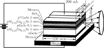
In 1970, Zh.I. Alferov and his collaborators Efim Portnoy, Dmitry Tretyakov, Dmitry Garbuzov, Vyacheslav Andreev, Vladimir Korolkov created the first semiconductor heterolaser operating in continuous mode at room temperature. Independently, Itsuo Hayashi and Morton Panish reported on the continuous lasing regime in lasers based on double heterostructures (with a diamond heat sink) in a paper sent to press only a month later. The continuous laser lasing mode at Fiztekh was implemented in lasers with stripe geometry, which were created using photolithography, and the lasers were installed on copper heat sinks coated with silver. The lowest threshold current density at room temperature was 940 A/cm 2 for wide lasers and 2.7 kA/cm 2 for strip lasers. The implementation of such a generation mode caused an explosion of interest. At the beginning of 1971, many universities and industrial laboratories in the USA, USSR, Great Britain, Japan, Brazil and Poland began researching heterostructures and devices based on them.
Theorist Rudolf Kazarinov made a great contribution to the understanding of electronic processes in heterolasers. The generation time of the first laser was short. Zhores Ivanovich admitted that he had just enough to measure the parameters necessary for the article. Extending the service life of lasers was quite difficult, but it was successfully solved through the efforts of physicists and technologists. Now, most owners of CD players are unaware that audio and video information is read by a semiconductor heterolaser. Such lasers are used in many optoelectronic devices, but primarily in fiber-optic communication devices and various telecommunication systems. It is difficult to imagine our life without heterostructure LEDs and bipolar transistors, without low-noise transistors with high electron mobility for high-frequency applications, including, in particular, satellite television systems. Following the heterojunction laser, many other devices were created, including solar energy converters.
The importance of achieving continuous operation of double heterojunction lasers at room temperature is primarily due to the fact that at the same time, low-loss optical fiber was created. This led to the birth and rapid development of fiber-optic communication systems. In 1971, these works were noted by awarding Zh.I. Alferov the first international award - the Ballantyne Gold Medal of the Franklin Institute in the USA. The special value of this medal, as noted by Zhores Ivanovich, lies in the fact that the Franklin Institute in Philadelphia awarded medals to other Soviet scientists: in 1944 to Academician P.L. Kapitsa, in 1974 to Academician N.N. Bogolyubov, and in 1981 to academician A.D. Sakharov. It is a great honor to be in such a company.
The awarding of the Ballantyne Medal to Zhores Ivanovich has a backstory connected with his friend. One of the first Physics and Technology students to come to the USA in 1963 was B.P. Zakharchenya. He flew around almost all of America, meeting with such luminaries as Richard Feynman, Carl Anderson, Leo Szilard, John Bardeen, William Fairbank, Arthur Schawlow. At the University of Illinois, B.P. Zakharchenya met Nick Holonyak, the creator of the first efficient gallium arsenide-phosphide LED emitting light in the visible region of the spectrum. Nick Holonyak is one of the leading American scientists, a student of John Bardeen, the only two-time Nobel Prize winner in the world in the same specialty (physics). He recently received an award as one of the founders of a new direction in science and technology - optoelectronics.
Nick Holonyak was born in the USA, where his father, a simple miner, emigrated from Galicia before the October Revolution. He brilliantly graduated from the University of Illinois, and his name is written in golden letters on a special “Honor Board” of this university. B.P. Zakharchenya recalled: “A snow-white shirt, a bow tie, a short haircut in the fashion of the 60s and, finally, an athletic figure (he lifted weights) made him a typical American. This impression was further strengthened when Nick spoke his native American language. But suddenly he switched to his father's language, and there was nothing left of the American gentleman. It was not Russian, but an amazing mixture of Russian and Ruthenian (close to Ukrainian), flavored with salty miner jokes and strong peasant expressions learned from their parents. At the same time, Professor Kholonyak laughed very contagiously, turning into a mischievous Rusyn guy before our eyes.”
Back in 1963, showing B.P. Zakharchena a miniature LED, shining brightly green, under a microscope, Professor Kholonyak said: “Marvel, Boris, at my suit. Nex time, tell them at your institute, maybe someone from your boys would like to come here to Illinois. I will teach him how to be a svitla.”

From left to right: Zh.I. Alferov, John Bardeen, V.M. Tuchkevich, Nick Holonyak (University of Illinois, Urbana, 1974)
Seven years later, Zhores Alferov came to Nick Kholonyak’s laboratory (being already familiar with him - in 1967 Kholonyak visited Alferov’s laboratory at the Physics and Technology Institute). Zhores Ivanovich was not the “lad” who needed to learn how to “be a gentleman.” I could teach myself. His visit was very successful: the Franklin Institute at that time was just awarding another Ballantyne medal for the best work in physics. Lasers were in vogue, and the new heterolaser, promising enormous practical prospects, attracted special attention. There were competitors, but the publications of Alferov’s group were the first. Support for the work of Soviet physicists by such authorities as John Bardeen and Nick Holonyak certainly influenced the commission's decision. It is very important in any business to be in the right place at the right time. If Zhores Ivanovich had not ended up in the States then, it is possible that this medal would have gone to competitors, although he was the first. It is known that “ranks are given by people, but people can be deceived.” Many American scientists were involved in this story, for whom Alferov’s reports on the first laser based on a double heterostructure were a complete surprise.
Alferov and Kholonyak became close friends. In the process of various contacts (visits, letters, seminars, telephone conversations), which play an important role in everyone’s work and life, they regularly discuss problems in the physics of semiconductors and electronics, as well as aspects of life.
The almost seemingly happy exception of the Al heterostructure x Ga 1– x As was subsequently expanded endlessly with multicomponent solid solutions - first theoretically, then experimentally (the most striking example is InGaAsP).

Space station "Mir" with solar batteries based on heterostructures
One of the first experiences of successful application of heterostructures in our country was the use of solar panels in space research. Solar cells based on heterostructures were created by Zh.I. Alferov and co-workers back in 1970. The technology was transferred to NPO Kvant, and solar cells based on GaAlAs were installed on many domestic satellites. When the Americans published their first works, Soviet solar panels were already flying on satellites. Their industrial production was launched, and their 15-year operation at the Mir station brilliantly proved the advantages of these structures in space. And although the forecast of a sharp reduction in the cost of one watt of electrical power based on semiconductor solar cells has not yet come true, in space the most efficient source of energy to this day is certainly solar cells based on heterostructures of A III B V compounds.
There were enough obstacles on Zhores Alferov’s path. As usual, our special services of the 70s. they didn’t like his numerous foreign awards, and they tried to prevent him from going abroad to international scientific conferences. Envious people appeared who tried to take over the matter and wipe Zhores Ivanovich away from fame and the funds necessary to continue and improve the experiment. But his entrepreneurial spirit, lightning-fast reaction and clear mind helped to overcome all these obstacles. “Lady Luck” also accompanied us.
1972 was a particularly happy year. Zh.I. Alferov and his student colleagues V.M. Andreev, D.Z. Garbuzov, V.I. Korolkov and D.N. Tretyakov were awarded the Lenin Prize. Unfortunately, due to purely formal circumstances and ministerial games, R.F. Kazarinov and E.L. Portnoy were deprived of this well-deserved award. In the same year, Zh.I. Alferov was elected to the USSR Academy of Sciences.
On the day the Lenin Prize was awarded, Zh.I. Alferov was in Moscow and called home to report this joyful event, but the phone did not answer. He called his parents (they had lived in Leningrad since 1963) and happily told his father that his son was a Lenin Prize laureate, and in response he heard: “What is your Lenin Prize? Our grandson was born!” The birth of Vanya Alferov was, of course, the greatest joy of 1972.
The further development of semiconductor lasers was also associated with the creation of a laser with distributed feedback, proposed by Zh.I. Alferov in 1971 and implemented several years later at the Physicotechnical Institute.
The idea of stimulated emission in superlattices, expressed at the same time by R.F. Kazarinov and R.A. Suris, was implemented a quarter of a century later in Bell Telephone. Research into superlattices, started by Zh.I. Alferov and co-authors in 1970, unfortunately, developed rapidly only in the West. Work on quantum wells and short-period superlattices in a short time led to the birth of a new field of solid-state quantum physics - the physics of low-dimensional electronic systems. The apogee of these works is currently the study of zero-dimensional structures - quantum dots. The work in this direction carried out by Zh.I. Alferov’s students of the second and third generations: P.S. Kop’ev, N.N. Ledentsov, V.M. Ustinov, S.V. Ivanov, has received wide recognition. N.N. Ledentsov became the youngest corresponding member of the Russian Academy of Sciences.
Semiconductor heterostructures, especially double ones, including quantum wells, wires and dots, are now the focus of two-thirds of semiconductor physics research groups.
In 1987, Zh.I. Alferov was elected director of the Physicotechnical Institute, in 1989 - chairman of the presidium of the Leningrad Scientific Center of the USSR Academy of Sciences, and in April 1990 - vice-president of the USSR Academy of Sciences. Subsequently, he was re-elected to these posts in the Russian Academy of Sciences.
The main thing for Zh.I. Alferov in recent years was the preservation of the Academy of Sciences as the highest and unique scientific and educational structure in Russia. They wanted to destroy it in the 20s. as “the legacy of the totalitarian tsarist regime,” and in the 90s. – as “the legacy of the totalitarian Soviet regime.” To preserve it, Zh.I. Alferov agreed to become a deputy in the State Duma of the last three convocations. He wrote: “For the sake of this great cause, we sometimes made compromises with the authorities, but not with our conscience. Everything that humanity has created, it has created thanks to science. And if our country is destined to be a great power, then it will be not thanks to nuclear weapons or Western investments, not thanks to faith in God or the president, but thanks to the work of its people, faith in knowledge, in science, thanks to the preservation and development of scientific potential and education." Television broadcasts of State Duma meetings have repeatedly testified to the remarkable socio-political temperament and ardent interest of Zh.I. Alferov in the prosperity of the country in general and science in particular.
Among other scientific awards of Zh.I. Alferov, we note the Hewlett-Packard Prize of the European Physical Society, the State Prize of the USSR, the Welker Medal; Karpinsky Prize, established in Germany. Zh.I. Alferov is a full member of the Russian Academy of Sciences, a foreign member of the National Academy of Engineering and the US Academy of Sciences, and a member of many other foreign academies.
Being the vice-president of the Academy of Sciences and a deputy of the State Duma, Zh.I. Alferov does not forget that as a scientist he grew up within the walls of the famous Physico-Technical Institute, founded in Petrograd in 1918 by the outstanding Russian physicist and organizer of science Abram Fedorovich Ioffe. This institute has given physical science a vibrant constellation of world-famous scientists. It was at the Physics and Technology Institute that N.N. Semenov conducted research on chain reactions, which was later awarded the Nobel Prize. Outstanding physicists I.V. Kurchatov, A.P. Aleksandrov, Yu.B. Khariton and B.P. Konstantinov worked here, whose contribution to solving the atomic problem in our country cannot be overestimated. The most talented experimenters - Nobel laureate P.L. Kapitsa and G.V. Kurdyumov, theoretical physicists of rare talent - G.A. Godov, Ya.B. Zeldovich and Nobel laureate L.D. Landau began their scientific activities at the Phystech. The name of the institute will always be associated with the names of one of the founders of the modern theory of condensed matter, Ya. I. Frenkel, and the brilliant experimenters E. F. Gross and V. M. Tuchkevich (who headed the institute for many years).
Zh.I.Alferov contributes to the development of Phystech as best he can. A Physics and Technology School was opened at the Physicotechnical Institute and the process of creating specialized educational departments on the basis of the institute continued. (The first department of this kind - the Department of Optoelectronics - was created at LETI back in 1973. On the basis of the already existing and newly organized basic departments, the Faculty of Physics and Technology was created at the Polytechnic Institute in 1988. The development of the academic education system in St. Petersburg was expressed in the creation of a medical faculty at the University and a comprehensive Scientific and Educational Center of the Physicotechnical Institute, which united schoolchildren, students and scientists in one beautiful building, which can rightfully be called the Palace of Knowledge. Using the opportunities of the State Duma for wide communication with influential people, Zh.I. Alferov “knocked out” money for the creation of a Scientific and Educational Center from each prime minister (and they change so often). The first, most significant contribution was made by V.S. Chernomyrdin. Now the huge building of this center, built by Turkish workers, stands not far from the Physics and Technology Institute, clearly showing what an enterprising person obsessed with a noble idea is capable of.
Since childhood, Zhores Ivanovich has been accustomed to speaking in front of a wide audience. B.P. Zakharchenya recalls his stories about the resounding success that he gained by reading from the stage almost in preschool age M. Zoshchenko’s story “The Aristocrat”: “I, my brothers, do not like women who wear hats. If a woman is wearing a hat, if she is wearing fildecos stockings...”
As a ten-year-old boy, Zhores Alferov read Veniamin Kaverin’s wonderful book “Two Captains” and for the rest of his life he followed the principle of its main character Sanya Grigoriev: “Fight and search, find and not give up!”
Who is he – “free” or “free”?
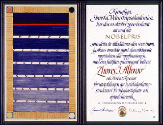

The Swedish king presents Zh.I. Alferov with the Nobel Prize
Compiled
V.V.RANDOSHKIN
based on materials:
Alferov Zh.I. Physics and life. – St. Petersburg: Nauka, 2000.
Alferov Zh.I. Double heterostructures: Concept and applications in physics, electronics and technology. – Uspekhi Fizicheskikh Nauk, 2002, v. 172, no. 9.
Science and humanity. International Yearbook. – M., 1976.


